Photonic chips leverage light to transmit information with minimal energy loss, enabling faster data processing and communication in optical networks. Plasmonic devices manipulate surface plasmons--electron oscillations at metal-dielectric interfaces--to achieve ultra-compact signal control beyond the diffraction limit. Explore the advancements and applications driving the future of photonic and plasmonic technologies.
Why it is important
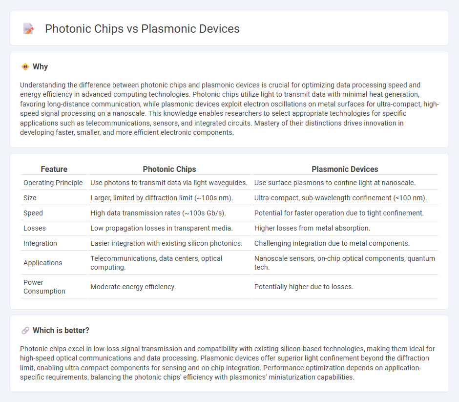
Understanding the difference between photonic chips and plasmonic devices is crucial for optimizing data processing speed and energy efficiency in advanced computing technologies. Photonic chips utilize light to transmit data with minimal heat generation, favoring long-distance communication, while plasmonic devices exploit electron oscillations on metal surfaces for ultra-compact, high-speed signal processing on a nanoscale. This knowledge enables researchers to select appropriate technologies for specific applications such as telecommunications, sensors, and integrated circuits. Mastery of their distinctions drives innovation in developing faster, smaller, and more efficient electronic components.
Comparison Table
| Feature | Photonic Chips | Plasmonic Devices |
|---|---|---|
| Operating Principle | Use photons to transmit data via light waveguides. | Use surface plasmons to confine light at nanoscale. |
| Size | Larger, limited by diffraction limit (~100s nm). | Ultra-compact, sub-wavelength confinement (<100 nm). |
| Speed | High data transmission rates (~100s Gb/s). | Potential for faster operation due to tight confinement. |
| Losses | Low propagation losses in transparent media. | Higher losses from metal absorption. |
| Integration | Easier integration with existing silicon photonics. | Challenging integration due to metal components. |
| Applications | Telecommunications, data centers, optical computing. | Nanoscale sensors, on-chip optical components, quantum tech. |
| Power Consumption | Moderate energy efficiency. | Potentially higher due to losses. |
Which is better?
Photonic chips excel in low-loss signal transmission and compatibility with existing silicon-based technologies, making them ideal for high-speed optical communications and data processing. Plasmonic devices offer superior light confinement beyond the diffraction limit, enabling ultra-compact components for sensing and on-chip integration. Performance optimization depends on application-specific requirements, balancing the photonic chips' efficiency with plasmonics' miniaturization capabilities.
Connection
Photonic chips utilize light to process and transmit data at speeds far exceeding traditional electronic circuits, while plasmonic devices harness surface plasmon resonances to confine light at the nanoscale, enhancing signal modulation and sensitivity. The integration of plasmonic components into photonic chips enables ultra-compact, high-speed optical communication systems with reduced energy consumption. This synergy accelerates advancements in data centers, telecommunications, and computing technologies by bridging the gap between photonics and nanoplasmonics.
Key Terms
Surface Plasmon Resonance
Surface Plasmon Resonance (SPR) in plasmonic devices enables highly sensitive detection of changes in the refractive index near metal-dielectric interfaces, surpassing conventional photonic chips in biosensing applications. Photonic chips primarily rely on dielectric waveguides, offering lower losses but limited sensitivity compared to the strong field confinement of plasmonic structures. Explore our detailed analysis to understand how SPR-based plasmonic devices revolutionize photonic technologies.
Waveguides
Plasmonic devices leverage surface plasmon polaritons to confine light beyond the diffraction limit, enabling ultra-compact waveguides with high field enhancement suitable for nanoscale photonic integration. Photonic chips utilize dielectric waveguides that offer low propagation loss and compatibility with silicon photonics, making them ideal for large-scale optical communication and signal processing applications. Explore detailed comparisons and cutting-edge research on waveguide technologies in plasmonic devices versus photonic chips to optimize future photonic systems.
Nanophotonics
Plasmonic devices leverage surface plasmon polaritons to confine light at the nanoscale, achieving superior field enhancement and enabling ultra-compact nanophotonic circuits compared to conventional photonic chips that rely on dielectric waveguides. Photonic chips excel in low-loss light propagation and integration with existing semiconductor technology, while plasmonic components offer breakthroughs in sensing, modulation, and nonlinear optics due to enhanced light-matter interactions. Explore the latest advances in nanophotonics to understand how these technologies complement and transform future optical communication and computing systems.
Source and External Links
Plasmonics - Wikipedia - Plasmonic devices manipulate optical signals at metal-dielectric interfaces on the nanometer scale, utilizing phenomena like surface plasmon polaritons for applications in sensing, microscopy, and optical communications.
What is Plasmonics? - AZoNano - These devices use metals such as gold and silver to concentrate light beyond the diffraction limit, enabling compact, highly sensitive optical sensors for environmental monitoring, food safety, and biological detection.
What Is Plasmonics? - Ansys - Plasmonic devices, including various nanoscale waveguides, allow chip-scale information processing at optical frequencies and are used in advanced sensors for detecting biological/chemical agents and improving LED efficiency.