Neuromorphic chips mimic the brain's neural architecture to enhance computing efficiency and enable advanced AI applications by processing data in parallel with low power consumption. In contrast, 3D stacked integrated circuits (ICs) vertically integrate multiple layers of semiconductor devices to boost performance, reduce latency, and save space. Explore the unique advantages and technological innovations behind neuromorphic chips and 3D stacked ICs to understand their transformative impact on next-generation computing.
Why it is important
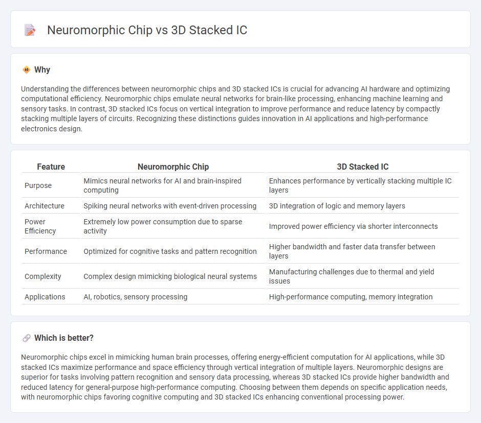
Understanding the differences between neuromorphic chips and 3D stacked ICs is crucial for advancing AI hardware and optimizing computational efficiency. Neuromorphic chips emulate neural networks for brain-like processing, enhancing machine learning and sensory tasks. In contrast, 3D stacked ICs focus on vertical integration to improve performance and reduce latency by compactly stacking multiple layers of circuits. Recognizing these distinctions guides innovation in AI applications and high-performance electronics design.
Comparison Table
| Feature | Neuromorphic Chip | 3D Stacked IC |
|---|---|---|
| Purpose | Mimics neural networks for AI and brain-inspired computing | Enhances performance by vertically stacking multiple IC layers |
| Architecture | Spiking neural networks with event-driven processing | 3D integration of logic and memory layers |
| Power Efficiency | Extremely low power consumption due to sparse activity | Improved power efficiency via shorter interconnects |
| Performance | Optimized for cognitive tasks and pattern recognition | Higher bandwidth and faster data transfer between layers |
| Complexity | Complex design mimicking biological neural systems | Manufacturing challenges due to thermal and yield issues |
| Applications | AI, robotics, sensory processing | High-performance computing, memory integration |
Which is better?
Neuromorphic chips excel in mimicking human brain processes, offering energy-efficient computation for AI applications, while 3D stacked ICs maximize performance and space efficiency through vertical integration of multiple layers. Neuromorphic designs are superior for tasks involving pattern recognition and sensory data processing, whereas 3D stacked ICs provide higher bandwidth and reduced latency for general-purpose high-performance computing. Choosing between them depends on specific application needs, with neuromorphic chips favoring cognitive computing and 3D stacked ICs enhancing conventional processing power.
Connection
Neuromorphic chips leverage 3D stacked IC technology to enhance computational efficiency by vertically integrating multiple layers of memory and processing units, mimicking neural networks in the human brain. This vertical stacking reduces interconnect latency and power consumption, critical for real-time AI applications. The synergy between neuromorphic architecture and 3D IC fabrication drives advancements in low-power, high-speed cognitive computing systems.
Key Terms
Through-Silicon Via (TSV)
Through-Silicon Via (TSV) technology plays a critical role in 3D stacked ICs by providing vertical electrical connections that enable higher integration density, reduced latency, and improved power efficiency compared to traditional 2D designs. Neuromorphic chips utilize TSVs to mimic brain-like architectures, achieving enhanced communication bandwidth and reduced interconnect length between neuron layers, which is crucial for real-time processing and low-power operation. Explore the advancements in TSV implementations to understand how they drive innovation in both 3D IC stacking and neuromorphic computing.
Spiking Neural Network (SNN)
3D stacked IC technology enhances neuromorphic chips by enabling dense vertical integration, which significantly improves the efficiency of Spiking Neural Networks (SNN) through reduced latency and energy consumption. Neuromorphic chips, designed to mimic brain-like spiking behaviors, benefit from 3D ICs by accommodating more synaptic connections and neuron models in a compact form factor. Explore in-depth how 3D stacked IC innovations advance SNN performance and applications.
Heterogeneous Integration
3D stacked IC technology enhances semiconductor design by vertically integrating diverse components such as logic, memory, and sensors, enabling heterogeneous integration and improved performance in compact form factors. Neuromorphic chips mimic neural architectures to process data efficiently, leveraging heterogeneous integration to combine analog and digital elements for low-power, high-speed computing. Explore the advancements in heterogeneous integration strategies driving the future of 3D stacked ICs and neuromorphic computing.
Source and External Links
What is 3D-IC Technology & Design - 3D-IC is a three-dimensional integrated circuit created by vertically stacking multiple chips or wafers into a single package, interconnected through through-silicon vias (TSVs) or hybrid bonding for higher functional density, lower power, and faster data transfer than traditional 2D designs.
Three-dimensional integrated circuit - A 3D IC stacks multiple integrated circuits vertically, using connections like through-silicon vias, to achieve improved performance, reduced power consumption, and a smaller footprint compared to conventional 2D ICs.
3D Integration and Stacked Wafers: The Future of ICs - 3D integration allows several layers of ICs to be stacked and connected vertically, enabling chips that are faster, smaller, more efficient, and capable of combining different functionalities in a compact form.
 dowidth.com